PALS Experimental Setup
Copyright © 1999, 2007 Kees Krijnen.
The experimental setup consist of (fig. 4) :
- Helium-Neon laser, wavelength 632.8 nm, to provide a coherent light source
- Beam expander and focus optics, to maximize scattering at crossing point
- Beam splitter and two mirrors to generate two equal laser beams in phase
- Glass tube at the crossing point of the two laser beams to measure sample
- Coherent detector - 200 µm pinhole, objective focus lens, 2nd pinhole and phototransistor
- AC amplifier to amplify intensity modulation from detector
- TMS320C542 DSP evaluation board with ADC
- 486 PC (DOS/WIN3.11) to monitor process and save data
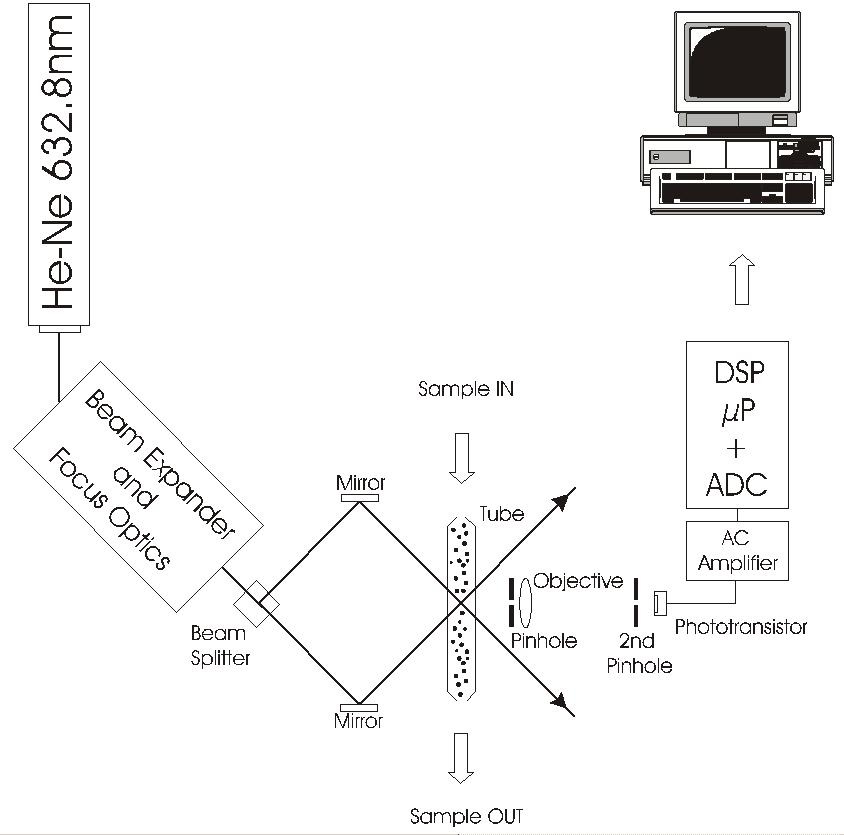
fig. 4. PALS Experimental setup.
The laser is a 5mW HeNe polarized laser from Melles-Griot, Carlsbad CA, USA. It requires a high voltage power supply (1.85-2.45kV, 6.5mA).
The tube is a cilindrical glass capillary, inner diameter 4 mm. The angle between the two laser beams, inside the tube, is affected by the difference in refractive index of medium inside and outside tube - Snell's law [14]. Sample is transported from reservoir to capillary via silicon tubes, and afterwards to waste.
Creamer solved in tap water has been used as test sample for PALS experiments, what provides a stable suspension. The concentration is chosen in such a way that the laser beams are clearly visible, there is no `glowing cloud' around the beams. As liquid transportation, gravity is used. The waste is lower than the sample reservoir. By varying the height of waste in respect to reservoir, different liquid flows can be set.
Instead of a photo multiplier tube a phototransistor is selected from UDT Sensors Inc., Hawthorne CA, USA. No specifications are known, but this phototransistor was applied in a system where extremely high sensivity for light was required.
The AC amplifier allows amplification from 1x to 500x to be selected by jumpers. The lower power supply ±5V of driver stage is meant to prevent overload of the ADC input; 6V differential load is allowed. OPA77 opamps were used, instead of OPA90. OPA90 is better suited for low power supply applications, but was not available. The driver stage OPA77 opamp shows some clipping for high negative outputs, but this has not affected results.
The TMS320C542 evaluation board (fig. 5) with TLC320AC01 14-bit ADC processes the signal from AC amplifier board. This DSP starter kit from Texas Instruments Inc. is supplied with DSKplus development board, C54x algebraic assembler, GoDSPs WindowsTM-based Code ExplorerTM debugger and various application programs.
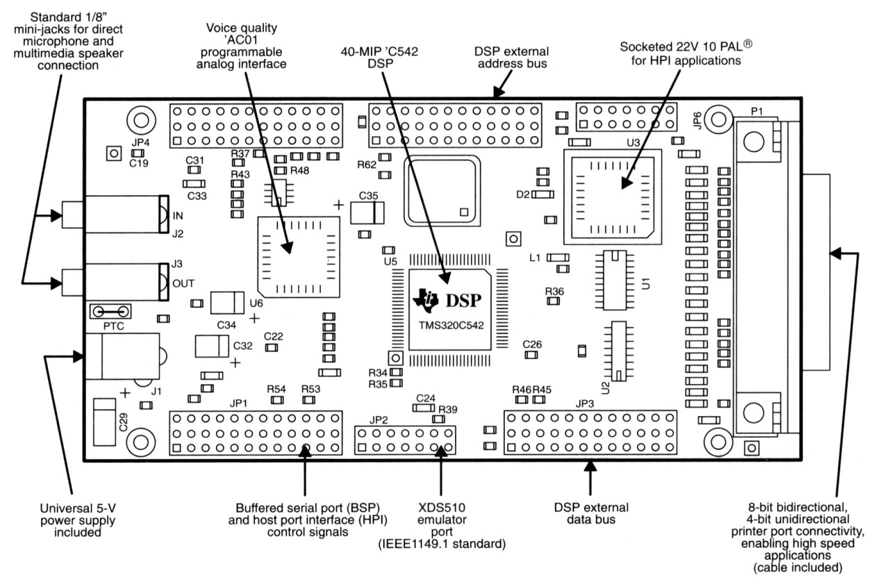
fig. 5. DSKplus Board Diagram (courtesy Texas Instruments Inc.)
Several features of the DSKplus board enable MIPS-intensive, low-power applications:
- One TMS320C542 enhanced fixed point DSP
- 40 MIPS (25-ns instruction cycle time)
- 10K words of dual-access RAM (DARAM)
- 2K words boot ROM
- One time-division-multiplexed (TDM) serial port
- One host port interface (HPI) for PC-to-DSP communications
- Programmable, voice-quality TLC320AC01 (DAC, ADC interface circuit)
The host port interface is an on-board PAL® device that operates as the main interface between the host PC parallel port and the C542 host port interface (HPI). As a result, the interface logic gives the host PC direct control of the C542 HPI and DSP reset signal, and it can configure the board to operate with different PC parallel ports (that is, 4-bit and 8-bit printer ports).
The C542 (fig 6.) has a high degree of operational flexibility and speed. It combines an advanced modified Harvard architecture (with one program memory bus, three data memory buses, and four address buses), a CPU with application-specific hardware logic, on-chip peripherals, and a highly specialized instruction set. Key features of C542 CPU, memory and instruction set are:
- Advanced multibus architecture with one program bus, three data buses, and four address buses
- 40-bit arithmetic logic unit (ALU), including a 40-bit barrel shifter and two independent 40-bit accumulators
- 17-bit x 17-bit parallel multiplier coupled to a 40-bit dedicated adder for nonpipelined single-cycle multiply/accumulate (MAC) operations
- Compare, select, store unit (CSSU) for the add/compare selection of the Vertibi operator
- Exponent encoder to compute the exponent of a 40-bit accumulator value in a single cycle
- Two address generators, including eight auxiliary registers and two auxiliary registers arithmetic units. Circular indexed addressing
- On-chip 2K ROM and 10K DARAM memory
- Single-instruction repeat and block repeat operations
- Block memory move instructions for better program and data management
- Instructions with a 32-bit long operand
- Instructions with 2- or 3-operand simultaneous reads
- Arithmetic instructions with parallel store and parallel load
- Conditional store instructions
- Fast return from interrupt
Separate program and data spaces allow simultaneous access to program instruction and data, providing a high degree of parallelism. For example, three reads and one write can be performed in a single cycle. Instructions with parallel store and application-specific instructions fully utilize this architecture. In addition, data can be transferred between data and program spaces. Such parallelism supports a powerful set of arithmetic, logic and bit-manipulation operations that can all be performed in a single machine cycle. Also, the C542 includes the control mechanism to manage interrupts, repeated operations, and fuction calling.
Features most important for the experimental setup are single-cycle multiplication with indexed addressing, circular indexed addressing and MAC operations.
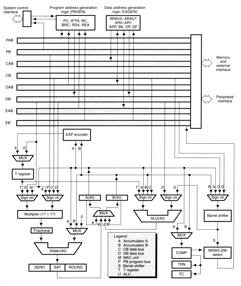
fig. 6. Block diagram C542 internal hardware (courtesy Texas Instruments Inc.)
The AC01 analog interface circuit (fig. 7) provides a single channel of voice-quality data acquisition. The AC01 has the following features:
- Single-chip solution A/D and D/A conversion with 14 bits of dynamic range
- Built-in, programmable antialiasing filter
- Software-programmable sampling rates
- Software-programmable reset, gain, and loopback
- Software-selectable auxiliary input
- 2nd-Complement 16-bit aligned Data Format
The AC01 interfaces directly to the C542 TDM serial port. The AC01 generates the required shift clock (SCLK) and frame sync (FS) pulses used to send data to/from the AC01. These pulses are a function of software-programmable registers and the AC01 master clock. The master clock (MCLK) is generated by the on-board 10 MHz oscillator.
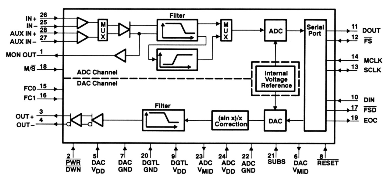
fig. 7. AC01 functional block diagram (courtesy Texas Instruments Inc.)
For convenient value reading a master clock (MCLK) of 10.368 MHz is assumed. All frequencies mentioned below and in Results chapter should be multiplied with 10/10.368 to get their real value!
Sampling frequencies of 2 kHz, 4 kHz and 8 kHz are applied. Their respective low-pass and high-pass filter frequencies are (B register value is default 18):
| 2 kHz - f(LP) = 900 Hz, 4 kHz - f(LP) = 1800 Hz, 8 kHz - f(LP) = 3600 Hz, |
f(HP) = 10 Hz, f(HP) = 20 Hz, f(HP) = 40 Hz, |
AC01 A reg. = 144 AC01 A reg. = 72 AC01 A reg. = 36 |
The f(LP)s match the Nyquist criteria. The minimum aquisition frame length used is 256 data points. Dividing the sampling frequency with this number gives the lowest extractable frequency - see full-cycle DFT/FFT requirement. The f(HP)s match as well, for example 8000/256 ± 31 Hz.